
Your SSPA's PCB doesn't match its schematic. This is confusing and feels wrong. Understanding why is key to building high-performance RF circuits that actually work in the real world.
The schematic is an ideal model, but a real-world PCB must account for high-frequency physics. At GHz frequencies, designers use physical microstrip lines as components and add features like grounding vias and decoupling capacitors to control parasitic effects and ensure stability, which aren't shown in the schematic.

When I started my career, I was looking at a finished PCB for a Solid State Power Amplifier. I noticed that the physical board looked very different from the circuit schematic I had studied. It felt like a map where the territory didn't match. This gap between the perfect drawing and the physical reality is where the real work of RF engineering happens. A perfect schematic is just the beginning. The real challenge is making that perfect idea work reliably on a physical board, and that requires changes that can seem strange at first. You need to understand these changes to build amplifiers that are stable, matched, and powerful.
Why Do Microstrip Lines Replace Components on a PCB?
You see a strange copper trace on the PCB. It’s not in the schematic. This isn't a mistake; it's high-frequency design in action, where traces become components themselves.
At frequencies above a gigahertz, lumped components like capacitors and inductors become unreliable1. Designers use precisely shaped microstrip lines on the PCB to act as distributed components2, providing predictable performance for tasks like impedance matching.

I will never forget an early experience in my career. I pointed to a Ka-band SSPA layout and asked my mentor, "Where did this microstrip line come from? It’s not in the schematic." His answer was a lesson I carry with me to this day. He explained that at low frequencies, we can use simple, "lumped" components like the capacitors and inductors you see in a schematic. But as the frequency climbs into the gigahertz range, those simple models fail. The physical size of the component starts to interact with the wavelength of the signal. So, we switch to a "distributed parameter model." Instead of a component, we use a copper trace with a specific length and width. This microstrip line is no longer just a wire; it is the inductor or capacitor, distributed along its length. This is essential for creating stable and matched high-power amplifiers.
| Model Type | Best For | How it Works | Example on PCB |
|---|---|---|---|
| Lumped Parameter | Low Frequencies (<1 GHz) | Uses discrete, ideal components (capacitors, inductors). | A small ceramic capacitor soldered to pads. |
| Distributed Parameter | High Frequencies (>1 GHz) | Uses physical geometry of traces to create circuit elements. | A specific length of microstrip line for matching. |
What Are Parasitic Effects and How Do You Tame Them?
Your perfect design is behaving erratically on the test bench. This is incredibly frustrating. The problem is likely invisible "parasitic" effects that only appear on the physical PCB.
Parasitics are unwanted inductance, capacitance, and resistance that are inherent in the physical layout of a PCB.3 They are managed with careful grounding, like adding dense arrays of "vias" to connect the ground planes and eliminate performance-killing resonance4.

My mentor taught me that a schematic is a perfect world, but a PCB lives in the real world with all its imperfections. At high frequencies, every trace, pad, and component lead has some unintended inductance and capacitance. We call these "parasitics." They don't appear on the schematic, but they can completely ruin your amplifier's performance. One of the most critical areas is grounding. A long, thin path to ground can act like an antenna, causing instability. To fight this, we add dense arrays of "vias," which are plated holes that stitch the top and bottom ground planes together. I remember seeing this on that first Ka-band amplifier. These vias create a very short, low-inductance path to ground5 right at the source of the transistor. This effectively short-circuits the parasitic effects, preventing unwanted feedback and ensuring the amplifier remains stable and performs as designed. It’s a physical solution to a physical problem.
How Do You Prevent an SSPA from Oscillating?
Your new amplifier is unstable and oscillating. This is a dangerous situation that can damage the device. You need a way to ensure stability directly on the PCB.
To prevent self-oscillation, designers add a series of decoupling capacitors right at the RF transistor's power pins6. These capacitors, arranged from small to large, filter out a wide band of frequencies, shorting unwanted noise to ground and stabilizing the circuit.
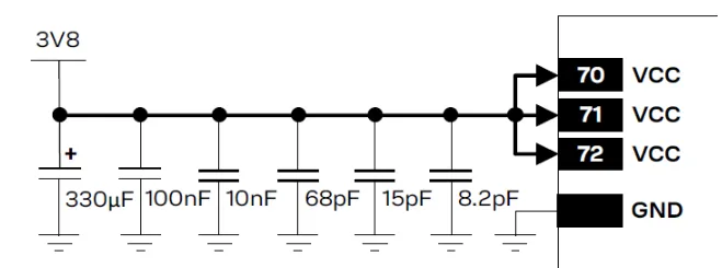
An amplifier, by its nature, wants to amplify. If any of its own output signal leaks back to its input with the right phase, it will start to amplify itself, creating a powerful and destructive oscillation. Schematics don't always show the full picture of how this can happen through the power supply lines. The solution, which I saw on that first SSPA board, is to place decoupling capacitors directly at the power pins of the active device. You can't just use one capacitor. The key is to use a range of them, placed physically from smallest to largest as you move away from the pin. Each capacitor has a "self-resonant frequency" (SRF) where it is most effective at shorting noise to ground.7
| Capacitor Size | Self-Resonant Frequency (SRF) | Main Purpose |
|---|---|---|
| Small (e.g., 100 pF)8 | High | Filters very high-frequency noise and harmonics. |
| Medium (e.g., 1 nF) | Medium | Filters noise in the main operating band. |
| Large (e.g., 1 uF) | Low | Provides a local energy reserve for low-frequency stability. |
By using this combination, we create a broadband filter that keeps the power supply clean and prevents the feedback that causes self-oscillation. This ensures the amplifier is stable and only amplifies the signals we want it to.
Conclusion
A successful SSPA is born when a perfect schematic is skillfully translated into a practical PCB, accounting for the real-world physics of high-frequency electronics.
"Transmission Lines: From Lumped Element to Distributed Element ...", https://www.allaboutcircuits.com/technical-articles/transmission-lines-from-lumped-element-to-distributed-element-regimes/. Research papers and textbooks on microwave engineering explain that as operating frequencies increase into the GHz range, the physical dimensions of lumped components become a significant fraction of the signal wavelength, leading to parasitic effects and self-resonance that make their behavior unpredictable. Evidence role: mechanism; source type: paper. Supports: That lumped components become unreliable above approximately 1 GHz because their physical size is no longer negligible compared to the signal's wavelength, causing them to exhibit unintended parasitic capacitance and inductance.. Scope note: The 1 GHz threshold is a general guideline; the exact frequency depends on the component size, substrate, and specific application. ↩
"[PDF] 1. introduction to distributed circuit design - UPCommons", https://upcommons.upc.edu/bitstreams/ee3bd237-8a32-4e0e-8e20-dd12841a36f1/download. Educational resources on RF and microwave engineering define distributed-element circuits, explaining how the geometry of transmission lines like microstrips can be precisely controlled to create predictable inductance, capacitance, and characteristic impedance for functions such as filtering and impedance matching. Evidence role: definition; source type: education. Supports: That microstrip lines, which are PCB traces with specific widths and lengths over a ground plane, can be designed to function as circuit elements like inductors, capacitors, and impedance matching networks at high frequencies.. ↩
"The New Chapter: The Impact of Parasitics on PCB Design", https://iconnect007.com/article/142055/the-new-chapter-the-impact-of-parasitics-on-pcb-design/142052/pcb. An encyclopedia or engineering handbook could define parasitic elements as the unintended electrical properties (inductance, capacitance, resistance) that arise from the physical implementation of a circuit, which are not part of the ideal schematic but can significantly affect performance, especially at high frequencies. Evidence role: definition; source type: encyclopedia. Supports: That parasitic elements are the unintended and unavoidable inductance, capacitance, and resistance that exist in electronic components and conductive traces due to their physical layout and proximity to other elements.. ↩
"Everything You Need to Know About Stitching Vias | PCB Layout", https://resources.altium.com/p/everything-you-need-know-about-stitching-vias. Application notes and research papers on high-speed PCB design demonstrate that creating a dense grid of vias between ground planes minimizes ground path inductance and suppresses the formation of resonant modes between the planes, which is critical for signal integrity and EMI control. Evidence role: mechanism; source type: paper. Supports: That adding dense arrays of grounding vias, often called 'via stitching' or 'via fencing,' connects the top and bottom ground planes to lower the ground path inductance and suppress parallel-plate waveguide modes or resonances that can degrade high-frequency circuit performance.. ↩
"Is There a Via Inductance Rule of Thumb? - Cadence System Analysis", https://resources.system-analysis.cadence.com/blog/msa2021-is-there-a-via-inductance-rule-of-thumb. Technical papers often provide models or measurements showing that the inductance of a typical PCB via is in the sub-nanohenry range, offering a significantly lower impedance path to ground at high frequencies compared to a longer routing trace on the PCB surface. Evidence role: statistic; source type: paper. Supports: That plated through-hole vias provide a much lower inductance path to a ground plane compared to a long surface trace, effectively 'shorting' the component to the ground plane at high frequencies.. Scope note: The exact inductance value depends on the via's dimensions (diameter, length) and the PCB stackup. ↩
"Decoupling capacitor - Wikipedia", https://en.wikipedia.org/wiki/Decoupling_capacitor. Application notes from semiconductor manufacturers and RF design guides recommend placing decoupling capacitors as close as possible to the power pins of an amplifier to provide a local, low-inductance source of charge and to shunt noise on the power supply line to ground, thereby preventing feedback that can lead to oscillation. Evidence role: general_support; source type: research. Supports: That placing a set of decoupling capacitors directly at the power supply pins of an active device like an RF transistor is a critical technique for ensuring stability by providing a low-impedance path to ground for high-frequency noise.. ↩
"Capacitor Self-resonant Frequency and Signal Integrity", https://resources.pcb.cadence.com/blog/2019-capacitor-self-resonant-frequency-and-signal-integrity. A source could explain that due to inherent equivalent series inductance (ESL), a real capacitor behaves like an RLC circuit and exhibits a self-resonant frequency (SRF) where its impedance is minimal; above this frequency, the capacitor's behavior becomes inductive. Evidence role: definition; source type: research. Supports: That a real-world capacitor has parasitic inductance (ESL) and resistance (ESR), causing it to have a self-resonant frequency (SRF) at which its impedance is at a minimum, making it most effective for filtering at that specific frequency.. ↩
"Decoupling Capacitor Calculations: What Size Should You Use For ...", https://resources.altium.com/p/what-size-decoupling-capacitor-should-i-use-my-digital-ics. A source could provide an example of a power delivery network design, showing that small-value capacitors (in the pF range) are chosen for their high self-resonant frequencies to filter high-frequency noise, while larger capacitors (in the uF range) act as local charge reservoirs to handle low-frequency current transients. Evidence role: case_reference; source type: research. Supports: That a common decoupling strategy involves using a small capacitor (e.g., 10 pF - 100 pF) for high frequencies, a medium capacitor (e.g., 1 nF - 100 nF) for mid-band noise, and a large bulk capacitor (e.g., 1 uF - 10 uF) for low-frequency current demands and stability.. Scope note: The specific values are exemplary and the optimal choice depends on the specific device, operating frequency, and PCB layout. ↩